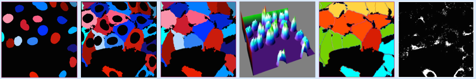
Photo Credit: Dr. Anne Carpenter
Join NESM for our annual Fall Symposium & Business Meeting on Thursday, November 20th at the Whitehead Institute in Cambridge, MA! The theme for our Symposium this year is "Building Microscopy Tools & Techniques." The meeting is designed to bring developers of microscopy tools together with researchers seeking new techniques to apply to their biological and materials science questions. The meeting will consist of five talks, a coffee break, a buffet dinner, and a business meeting in which elections will be held for several positions on the Board of Directors. Election ballots will be distributed with the Fall E-Newsletter.
Our schedule can also be found on our meeting flyer. Feel free to download, print, and post the flyer around your institution. We appreciate the extra advertising!
MEETING FLYER
Meeting Schedule
1:00 PM – Registration
1:30 PM – Welcoming Remarks - Blair Rossetti, President 2014
1:45 PM – “Electron Induced Near Field Optical Microscopy for Plasmonic Nanostructures” , Jun Xu, PhD, Massachusetts Institute of Technology
2:25 PM – "Stable and monodisperse membrane labeling of neurons with bright nitrogen vacancy nanodiamonds in-vitro and in the live mouse brain", Or Shemesh, PhD, MIT Media Lab
3:05 PM – Coffee Break
3:45 PM – "DNA probes for highly multiplexed,
precisely quantitative, ultra-resolution imaging
", Peng Yin, PhD, Wyss Institute
4:25 PM – "Extracting rich information from biological images to tackle world health problems", Anne Carpenter, PhD, Broad Institute
5:05 PM – Discussion Break
5:20 PM – Keynote - "Building advanced scientific apparatus quickly and at low cost", Ben Krasnow, Google X
6:20 PM – Buffet Dinner
7:30 PM – Business Meeting
8:30 PM – Closing Remarks - Jennifer Ross, PhD, President 2015
Additional Speaker Information
“Electron Induced Near Field Optical Microscopy for Plasmonic Nanostructures” , Jun Xu, PhD, Massachusetts Institute of Technology
Abstract:
Recently, low-energy excitation by swift electrons has been applied to explore the optical response of nanostructured materials with unmatched spatial resolution. For example, the measurement of photon emission rate using cathodoluminescence techniques can provide a direct quantification of local radiative energy transfer from electron to photons at spot size close to 10 nanometers, which compliment other experimental techniques such as photoluminescence. Such tightly localized excitation source and a high-resolution mapping technique is particularly suited to study the spontaneous emission rate of a plasmonic nanostructure with sub-wavelength mode volume. In this talk, we show that dark plasmons in metal nanoantenna and nanocavities can strongly enhance the interaction between moving electron and photon even though dark plasmon itself interacts weakly with photon. Such a counterintuitive experimental result is well-explained by our model based on eigen-response theory as well as numerical simulations. Our finding may offer new opportunity to improve single-photon emission and detection in nanostructures.
Bio:
Jun Xu is currently a Research Scientist at the Department of Mechanical Engineering, MIT. He received his PhD degree in Physics from the Hong Kong University of Science and Technology in 2007, and Bachelor’s degree in Physics from Fudan University in China, 2001. Before joining MIT, he was a post-doctoral research associate in the Department of Mechanical Science and Engineering, University of Illinois at Urbana-Champaign. With his expertise in fabrication and characterization of large scale 3D photonic quasicrystal and holographic lithography, he has explored the enhanced light-matter interaction in the subwavelength scale by plasmonic nanostructures. Dr. Xu’s current research interests span from manipulating the electromagnetic wave and acoustic wave by using metamaterials to their novel applications by the implementation of the new physics in materials science, biomedicine, and energy.
"Stable and monodisperse membrane labeling of neurons with bright nitrogen vacancy nanodiamonds in-vitro and in the live mouse brain", Or Shemesh, PhD, MIT Media Lab
Abstract:
Voltage imaging in the live brain demands both bright and sensitive sensors. In this regard, nitrogen vacancy (NV-NDs) nanodiamonds are good candidates since they serve as sensors for magnetic and electric fields and are extremely bright (~10 6 p/s) and small (down to 5nm). To achieve efficient sensing of voltage the NV-NDs have to be either close (within a Debye length) or anchored in the membrane bilayer. However, nanodiamonds tend to clump in solution and to endocytose after coming in contact with the membrane. To increase monodisperity and affinity to the membrane, we first rendered 40 and 100nm NV-NDs hydrophobic by coating them with a thin (1-5nm) layer of trimethoxy(octyl)silane, verified by transmission electron microscopy, EDX and FTIR. The functionalized nanodiamonds were stable in toluene. To deliver the hydrophobic nanodiamonds to neuronal membranes, we encased them in micelles composed of phosphoethanolamine conjugated to a PEG group (PEG-PE). Following a 10 minute incubation of micellated nanodiamonds with hippocampal neurons, single bright puncta were readily observed on the neurons. These NDs followed the morphology of neurons, from soma through small neurites. Membrane labeling with commercially available WGA-488 demonstrated that the diamonds reside in close proximity to the membrane, and confocal imaging revealed that the nanodiamonds were stable on the neuronal membrane without endocytosis for 6-12 hours from incubation, longer than membrane dyes. Using TEM and SEM of NDs on neurons we found that hydrophobic NDs come in contact with the membrane and form a monodisperse layer on it while hydrophilic NDs form micron-size aggregates in and on and off cells. Two photon imaging in culture and in live mouse brains showed that while hydrophilic NDs tend to be retained at the site of injection, micellated hydrophobic NDs can effectively label neurons. Both patching and propidium-iodide staining experiments showed that ND labeled neurons are live and physiologically functional. To conclude, we achieved membrane labeling with monodisperse, stable and bright NV-NDs, which can label neurons in-vitro or in the living brain and will serve as a prerequisite for any nanodiamond-based sensing. We are now quantifying voltage sensitivity of these NV-NDs in live spiking neurons.
Bio:
Or is a neuroscientist with a penchant for nanotechnology. He joined the synthetic neurobiology group in MIT after working with silicon nanowire transistors adapted for in-vivo brain recording at Harvard University. Or obtained his PhD from Hebrew University of Jerusalem where he studied Alzheimer’s disease using an invertebrate neural culture model he developed. In MIT, Or is interested in designing innovative tools to study the activity of many neurons simultaneously in the living brain. He uses both engineering and genetic methodologies to reach this end. His previous research and academic expertise include biology, psychology and electrical-engineering.
"DNA probes for highly multiplexed,
precisely quantitative, ultra-resolution imaging" Peng Yin, PhD, Wyss Institute
Abstract:
Living organisms are complex molecular systems. Imaging provides a natural and direct way to investigate such systems and is thus becoming a central tool for biomedical science. However, due to limitations of current microscopy, scientists face three crippling changes when attempting to visualize biology on the molecular scale: blurred vision (i.e. inability to visualize individual molecules clearly, especially for crowded targets), (partial) color blindness (i.e. only a small number [typically 3 or 4] of colors are used to simultaneously track distinct molecular species), and ambiguous quantification (i.e. inability to precisely count the number of target molecules in a resolution limited area). Using programmable fluorescent DNA probes (Nature Methods, 11:313, 2014; Science 344:65, 2014), we present a highly multiplexed (10× demonstrated), precisely quantitative (>90% precision), and ultra-high resolution (sub-5 nm) optical imaging method that simultaneously addresses these challenges, and hence promises to broadly transform biomedical research.
"Extracting rich information from biological images to tackle world health problems", Anne Carpenter, PhD, Broad Institute
Abstract:
Microscopy images contain rich information about the state of cells, tissues, and organisms and are an important part of experiments to address a multitude of basic biological questions and world health problems. Our laboratory works with dozens of collaborators around the world to design and execute large-scale microscopy-based experiments in order to identify the causes and potential cures of disease. The open-source software we produce, CellProfiler, is constantly improved based on these projects. For example, we recently added a Worm Toolbox for analysis of C. elegans, and machine-learning tools allow a biologists’ intuition to guide the computer to measure subtle phenotypes. The latter is particularly helpful in analyzing co-cultured cell systems. Although CellProfiler was designed and refined through high-throughput microscopy experiments, it is readily usable for quantifying information in small-scale experiments, too (www.cellprofiler.org).
Bio:
Dr. Carpenter leads the Imaging Platform at the Broad Institute of Harvard and MIT, a team of biologists and computer scientists who develop image analysis and data mining methods and software that are freely available to the public through the open-source CellProfiler project. She collaborates with dozens of biomedical research groups around the world to help identify disease states, potential therapeutics, and gene function from microscopy images. Carpenter is a Massachusetts Academy of Sciences fellow, an NSF CAREER awardee, and has also been funded by the NIH, Human Frontiers in Science, and the Howard Hughes Medical Institute.
"Building advanced scientific apparatus quickly and at low cost", Ben Krasnow, Google X
Abstract:
There are three major factors that have made it possible to build a scanning electron microscope, X-ray backscatter imaging system, X-ray CT scanner, Raman spectrometer, and custom LCD among other advanced prototypes, in a small shop on a hobbyist budget. These factors are: crowdsourcing of tools and information, availability of parts and tools via a growing second-hand market, and low-barrier access to patents and academic papers. As the availability of physical goods and information increases, it will be easier for hardware engineers to build very advanced systems without the expense and long lead times associated with getting help from an established industry source. The shorter, iterative development cycle coupled with the low cost of this experimentation allows for a new style of innovation that will increasingly compete with more traditional methods.
Bio:
After graduating with a BS in mechanical engineering from UCSB in 2005, Ben founded Mag Design and Engineering, a company that designed and built custom hardware for use in brain imaging studies. In many cases, this hardware was a computer peripheral, such as a keyboard or mouse, which was designed to be used within a Magnetic Resonance Imaging scanner. Ben also participated in related academic research at the Stanford Psychiatry Neuroimaging Lab. In 2011, Ben joined Valve Software, a popular computer gaming company in Seattle that sought expertise to launch a new hardware division. While at Valve, Ben developed an advanced Virtual Reality prototype headset among other game input devices. In 2014, Ben joined Google[x] and works on undisclosed projects there. Throughout his career, Ben has maintained a personal Youtube channel ("Applied Science") in which he posts videos of electromechanical and science projects done in his home workshop.
Location
McGovern Auditorium
Whitehead Institute
9 Cambridge Center
Cambridge, MA 02142
Parking
The Whitehead Institute is in the heart of Kendall Square/MIT and is within easy access of the Red Line T and bus routes.
- Traffic can be tough in Kendall Square so, if you decide to drive, please check Google directions to allow sufficient time.
- The map at http://en.parkopedia.com/parking/kendall_sq_cambridge/ shows local parking options. Whitehead Institute is located at the intersection marked with the location pin and the metered street parking pin.
- Street parking is limited to two hours and Cambridge Police are diligent in enforcing that.